


High electronic couplings of single mesitylene molecular junctions
Nov 7,2019
Abstract
We report on an experimental analysis of the charge transport properties of single mesitylene (1,3,5-trimethylbenzene) molecular junctions. The electronic conductance and the current–voltage characteristics of mesitylene molecules wired into Au electrodes were measured by a scanning tunnelling microscopy-based break-junction method at room temperature in a liquid environment. We found the molecular junctions exhibited two distinct conductance states with high conductance values of ca. 10−1G0 and of more than 10−3G0 (G0 = 2e2/h) in the electronic conductance measurements. We further performed a statistical analysis of the current–voltage characteristics of the molecular junctions in the two states. Within a single channel resonant tunnelling model, we obtained electronic couplings in the molecular junctions by fitting the current–voltage characteristics to the single channel model. The origin of the high conductance was attributed to experimentally obtained large electronic couplings of the direct π-bonded molecular junctions (ca. 0.15 eV). Based on analysis of the stretch length of the molecular junctions and the large electronic couplings obtained from the I–V analysis, we proposed two structural models, in which (i) mesitylene binds to the Au electrode perpendicular to the charge transport direction and (ii) mesitylene has tilted from the perpendicular orientation.

Introduction
Along with increasing interests in molecular electronics on the single molecular scale [1], much efforts have been devoted to understand charge transport in a single molecular junction, in which a single molecule is wired to two metal electrodes. In recent years single molecular junctions with electronic functionalities such as diodes [2-8] and transistors [9-13] have been demonstrated. Electronic conductances for most of the single molecular junctions were reported to be below 0.01G0 (G0 = 2e2/h, G0−1 ≈ 12.9 kΩ). The low electronic conductances prevent practical application of the molecular junctions for the molecular electronics. To bind a single molecule to metal electrodes, anchoring groups such as –SH [14] and –NH2 or (R)3–N [15,16] have been used. Such anchoring groups form strong chemical bonds with metal electrodes and the anchoring regions act as resistive space, leading to low electronic conductances of the single molecular junctions. Recently several groups [17-20] including ours [17,21,22] developed a direct π-binding technique, where a π-conjugated molecule is directly bound to metal electrodes without anchoring groups. The direct π-binding technique has been applied for various systems such as benzene derivatives [17,19,20], C60 [23,24], ethylene [25], and pyrazine [22,26]. The conductance values of these molecular junctions were close to those of metal atomic contacts. The high electronic conductance is expected to be caused by effective metal–molecule couplings in the direct π-binding to the electrodes. However, there are little direct experimental results revealing strong metal–molecule couplings.
The electronic structure of molecular junctions including metal–molecule couplings can be characterized by current-voltage (I–V) characteristics of molecular junctions. Transition voltage spectroscopy [27,28] is one of the methods to characterize energy level of conduction orbitals in junctions by analysing I–V characteristics. Energy level alignment of conduction orbitals with respect to Fermi level of metal electrodes has been examined for the molecular junctions of alkanedithiol, 1,4-benzenedithiol (BDT) and other molecules [29-31]. Recently I–V curve analysis [32] based on the Breit–Wigner model [33-37] has been becoming a promising technique to characterize the metal–molecule couplings of the single molecular junctions. Within the Breit–Wigner model, electronic conductance of the single molecular junction can be described by two parameters of (i) the electronic coupling between electrodes and molecule and (ii) the relative energy level alignment of the conduction orbital of molecule with respect to the Fermi level of the metal electrodes. By fitting the experimentally obtained I–V characteristics to the Breit-Wigner model, the metal–molecule coupling Γ, and energy difference between Fermi level and conduction orbital ε0 are obtained. This I–V analysis has been applied for molecular junctions with a variety of anchoring groups. For example Γ = 60 meV and ε0 = 0.6 eV have been reported for BDT [37], and Γ = 6 meV and ε0 = 0.5 eV for thiolated oligo(phenylene ethynylene) [36].
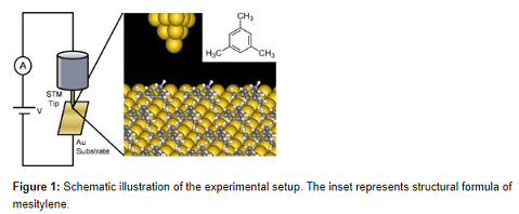
In this study, we report on the I–V analysis for the direct π-bonded molecular junction system without anchoring groups, i.e., mesitylene molecular junctions (Figure 1) to characterize Γ as well as ε0. Very recently Afsari et al. have investigated the single mesitylene molecular junction with a scanning tunnelling microscopy (STM)-based break junction (BJ) technique [20]. The conductance of a single mesitylene molecular junction has been founded to be approximately 0.1G0, which is at least 10 times larger than di-substituted benzene such as BDT [38] and 1,4-benzenediamine (BDA) [16]. The mesitylene molecule can bind to metal electrodes with its molecular plane perpendicular to the direction of charge transport [20]. Here, we investigate the possible origin of the high conductance of the direct π-bonded system. By analysing the I–V characteristics of the mesitylene junctions, we demonstrate that the direct π-bonded system features larger metal–molecule coupling.
Results and Discussion
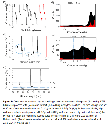
Mesitylene molecular junctions sandwiched by Au electrodes were prepared by the BJ method [39]. We used the STM-BJ method [15] operating in a liquid environment where thousands of molecular junctions were repeatedly made for statistical analysis of the molecular conductance and I–V characteristics. Figure 2 shows the conductance traces and histograms during stretching processes of the junctions. In the presence of the molecule, the conductance traces display plateaus at 1G0, and the corresponding conductance histograms show a peak at 1G0 (Figure 2a,d). These results indicate that a single Au atomic contact of 1G0 is formed at the initial stage of the stretching process. This suggests that nano-sized (atomic scale) Au electrodes are repeatedly made just after the rupture of the Au contact to trap a single mesitylene. At the conductance range below 1G0, conductance steps preferentially appeared around 0.1G0 and 0.03G0 (Figure 2b,c), which are absent in blank measurements. Conductance histograms show molecular conductance-peaks around 0.1G0 and 0.03G0. We observed two distinct high and low conductance states for a mesitylene junction. In a thousand of measured conductance traces, a small number of traces exhibit switch between the two states. The preferential conductance peaks around 0.1G0 agrees with the previously reported results by Afsari et al. According to [20], this conductance corresponds to single molecular junctions where mesitylene binds to Au electrodes with its molecular plane perpendicular to the charge transport direction. It should be noted that a side-peak at 0.2G0 is noticeable in Figure 2e, which is possibly due to formation of multi-molecular junctions. In our conductance measurement, plateaus are also present around 0.03G0. In STM-BJ experiments, molecular conductance appears as integer multiple plateaus of a fundamental molecular conductance [15] and the fundamental conductance corresponds to the single molecular conductance. Hence, this peak also represents the single molecular conductance of mesitylene junction. In our previous report [40], we have performed STM-BJ experiments on BDA in the mesitylene solution. It has been demonstrated that anime-derivatives form self-assembled adlayer on Au surface [41,42]. In the presence of BDA, both surfaces of the Au tip and Au substrate were covered by BDA in the mesitylene solution. Therefore BDA junctions can preferentially form in the 10 mM BDA mesitylene solution in our previous study. In [20], conductance analysis has been performed using linear-binned histograms and the low conductance state (0.03G0) found in the present study can be hidden in background tunnelling currents.
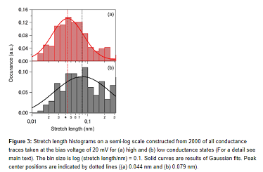
To estimate the effective separation of electrodes for the high-conductance and the low-conductance state, we analysed the electrodes separation length in the conductance traces. Figure 3 shows length histograms of the two types of conductance steps. The step length (i.e., the stretch length after the breakage of Au atomic contact) is defined as length of conductance plateau within the conductance range from 0.07G0 to 0.7G0 for the high-conductance state and from 0.02G0 to 0.7G0 for the low-conductance state. Gaussian fits of the length distribution reveal average step lengths of 0.044 and 0.079 nm for high- and low-conductance states, respectively. The stretch length of the low-conductance state is larger than that of the high-conductance state. It should be noted here that the length does not directly correspond with the actual gap size. The breakage of the Au atomic contact leads to the immediate formation of a nanogap of finite size as a result of the elastic response of the electrode banks. In case of Au atomic contact, the width of the gap thus created is typically 0.4 nm [43]. Considering that mesitylene binds to the Au electrodes with its molecular plane perpendicular to the charge transport direction [20] for the high conductance state of 0.1G0, the larger stretch length for the low state of 0.03G0 can be interpreted as a result of tilted orientation of the mesitylene junction upon stretching. We will discuss this matter in a later section.
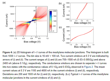
We examined I–V characteristic to obtain the electronic couplings of single molecular junction. In previous research [20], the current-versus-bias relationship of mesitylene junctions has been investigated by repeating current measurement at fixed bias voltages under 0.3 V. It has been reported that the current increases quasi-linearly with the bias voltage at the low bias regime. In this study we measured I–V characteristics of the mesitylene junctions by sweeping a wide bias range of ±1 V at fixed electrode separations. Figure 4 shows a 2D histogram and typical I–V curves of mesitylene molecular junctions. In addition to the almost linear increase of the current at low bias voltages, a non-linear increase of the current is apparent at high bias voltages. In the high-bias range, the Fermi level of the Au electrode moves close to the energy levels of the mesitylene conduction orbitals. Thus, the charge transport changes from non-resonant to resonant transport. Two clear distributions are present in the 2D histogram (Figure 4a). This result is in agreement with the two states (high and low sates) in the STM-BJ conductance measurement (Figure 2). To obtain statically averaged I–V curves for the two states, the current windows of 700–1500 nA (0.03–0.065G0) and above 2400 nA (above 0.1G0) at +0.3 V are selected for low and high states, respectively. The conductance windows are chosen to separate the I–V curves into two states with the conductance values of 0.1G0 and 0.03G0 observed in Figure 2.
We fabricated single molecular junctions of mesitylene with the STM-BJ method and performed conductance and I–V measurements. In the conductance measurement and I–V measurement, two conductance states (a high-conductance and a low-conductance state) were identified. The energy level alignment and the electronic couplings of mesitylene to Au electrodes were determined by fitting of statistically averaged I–V curves. The origin of the high conductance for the direct π-bonded molecular junctions was ascribed to the experimentally obtained large electronic couplings of ca. 0.15 eV for the two states. Based on the stretch length of the conductance trace and the large electronic coupling obtained from the I–V analysis, we proposed two structural models.
Experimental
Conductance measurements were performed using an electrochemical scanning tunnelling microscope (Nanoscope V, Bruker, Santa Barbara, CA). Au(111) substrate was prepared by thermal deposition of Au on cleaved mica surface at 625–675 K. The Au substrate was cleaned by flame annealing before use. Then the Au substrate was fixed in a Teflon liquid cell with the Viton O-ring. Pure mesitylene solvent was poured into the cell. STM-BJ experiments were performed as reported previously. The STM tip was prepared by mechanically cutting Au wire (diameter = 0.3 mm, purity >99%) [45]. In the I–V experiments, the STM tip was approached to the substrate until a metal junction with conductance of 6.5G0 was formed in air at room temperature. Subsequently, the tip was withdrawn for 10 nm at a tip speed of 38 nm/s to break the Au junction and to prepare the molecular junction. The tip was held and the bias voltage was simultaneously swept at 100 kHz frequency to record one I–V curve. The bias voltage range was ±1 V. Then, the junction was broken by pulling away of the tip from the substrate. We repeated this process and obtained more than 1000 I–V curves. The I–V characteristics of molecular junction were obtained by removing I–V curves of Au junctions or vacuum gaps. The I–V curves for the vacuum tunnelling are defined as I–V curves with less than 100 nA current at a bias of 1 V (ca. 0.0013G0) while I–V curves with less than 10000 nA current at a bias of 0.2 V (ca. 0.65G0) were assigned to charge transport through metal contacts. More than 95% of the I–V curves recorded in blank experiments fall into either the vacuum tunnelling or the charge transport through metal contacts.
- Related articles
- Related Qustion
- An investigation into the toxicity of mesitylene May 8, 2024
The effects of mesitylene on health, mainly developmental or neurological toxicity, were evaluated only in vitro and epidemiological studies
- Mesitylene: Applications in various fields Jul 21, 2023
Mesitylene's versatility and unique properties have positioned it as a valuable compound in various fields.
Olivetol, also known as 5-pentylresorcinol or 5-pentyl-1,3-benzenediol, is an organic compound found in certain species of lichen; it is also a precursor in various syntheses of tetrahydrocannabinol.....
Nov 7,2019Organic Synthesis Intermediate
These reagents are prepared by the reaction between diisobutylaluminium hydride and selenium or tellurium powders. They are obtained as a mixture of (Bui 2AlE)2 and (Bui AlE)n where E is Se or Te.....
Nov 7,2019Organic Chemistry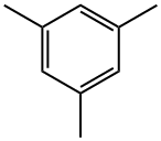
Mesitylene
108-67-8You may like
- Mesitylene
-

- $2.00 / 25kg
- 2025-12-12
- CAS:108-67-8
- Min. Order: 1kg
- Purity: ≥99%
- Supply Ability: 1000mt/year
- Mesitylene
-

- $0.00 / 1KG
- 2025-12-11
- CAS:108-67-8
- Min. Order: 1KG
- Purity: 99%
- Supply Ability: 10 mt
- Mesitylene(1,3,5-Trimethylbenzene)
-
- $75.00 / 1KG
- 2025-10-14
- CAS:108-67-8
- Min. Order: 100g
- Purity: >99%
- Supply Ability: 300tons